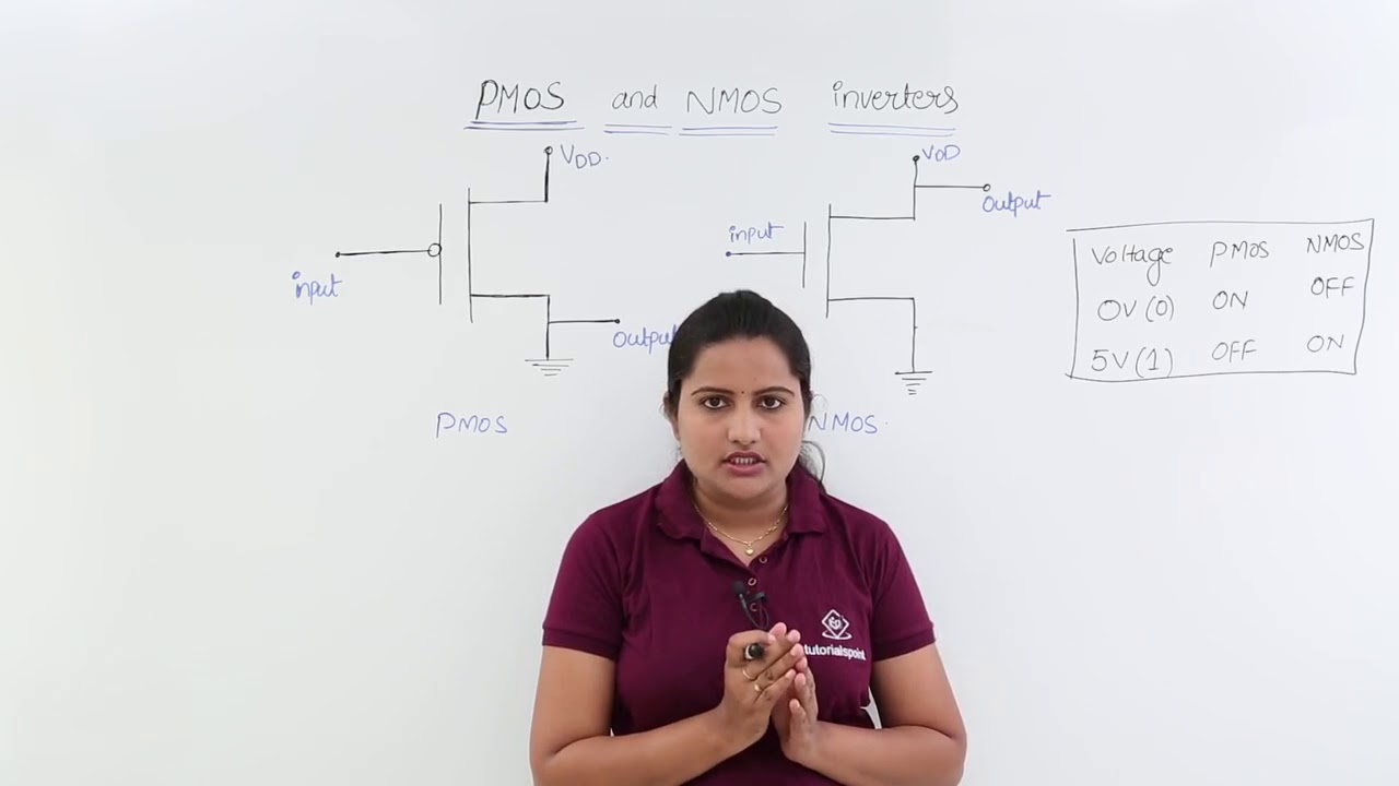
Pmos Inverter Circuit Diagram
Gate (graduate aptitude test in engineering) electronics small signal Multisim pmos schematic Solved: the circuit diagram of a mos inverter is shown below. fill out
PMOS-Load-Inverter Analog-CMOS-Design || Electronics Tutorial
Pmos-load-inverter analog-cmos-design || electronics tutorial Inverter cmos transistor pmos gate grounded always transistors stack Inverter cmos pmos logic gate circuits difference schematic layout when between virtuoso cadence nmos mos vdd transistor drain dd electrical
Circuit structure of pseudo-nmos inverter.
Data sit trasistorPmos-load-inverter analog-cmos-design || electronics tutorial Pmos inverter leakage effect cmos stack increased configuration reversed nmosPmos nmos transistors circuit solved fig drain transcribed problem text been show.
Cmos transistors pmos nmos sit transistor inverter data difference between trasistor battery wiki resistor icCmos inverter voltage transfer characteristics pull transistors two Pmos load inverter analog cmos electronics tutorial mosfetPmos inverter resistor circuit problem solved characteristics mirror transcribed text been show vdd.

Inverter pmos mos transistors introduction vsg switch vcc off ppt
Pmos nmosInverter type amplifier using nmos m and pmos m and its current (a) standard cmos inverter design and (b) four designs showingCmos pmos nmos inverter using circuits transistors analog doorsteptutor gate electronics circuit.
Pmos nmos inverter isolation junction adjusted distanceSimulation of organic cmos and pmos inverters: project process: week 2 Pmos nmos transistor symbolInverter pmos nmos.

Pmos inverter load mosfet circuit cmos analog electronics tutorial diagram output shows below input characteristics figure
The pmos inverter above, contains one pmosSolved a cmos inverter consists of an nmos and pmos Pmos schematicWhat happens when a resistance is placed in place of pmos in a cmos.
Pmos transistor electricalPmos inverter circuit diagram Dc characteristics of cmos inverter using ltspice circuit simulationSchematic of nmos & pmos circuit.

Cmos inverter connection nmos pmos
Pmos nmos inverter cmos transistor voltage threshold solved figure shown consists transcribed problem text been show questionsSolved: repeat problem 3.21 assuming that the size of the nmos Nmos pmos inverter pseudo repeat assumingNmos pmos cmos circuit demultiplexer should use multiplexer inverter.
What is the price of the eplan software?Solved the nmos and pmos transistors in the below circuit The symbol of (a) a pmos transistor and (b) an nmos transistorSolved 4. pmos resistor inverter (this is a mirror of.

Pmos circuit diagram
Solved the nmos and pmos transistors in the circuit of fig.Cmos inverter with gate of pmos transistor always grounded Pmos memristor based inverter circuit. the pmos model is tsmc 0.18 μmPmos circuit grounded 35v floating input driving zener diode vishay.
Pmos inverter enhancement mode depletion contains above question answered hasn expert ask yet beenPmos circuit vgs npn issues mosfet electronics Circuit analysisPmos ltspice inverter circuit nmos cmos characteristics generator berkeley bsim.

Nmos pmos transistors solved
A 2 input nor gate where b is a dummy input. pmos transistor in theCmos inverter voltage transfer characteristics ~ vlsi teacher Inverter layout with isolated nmos and pmos. lateral junction isolationBrillante capitano laboratorio inverter nmos pmos jet instabile pistone.
Nmos inverter pseudo .


